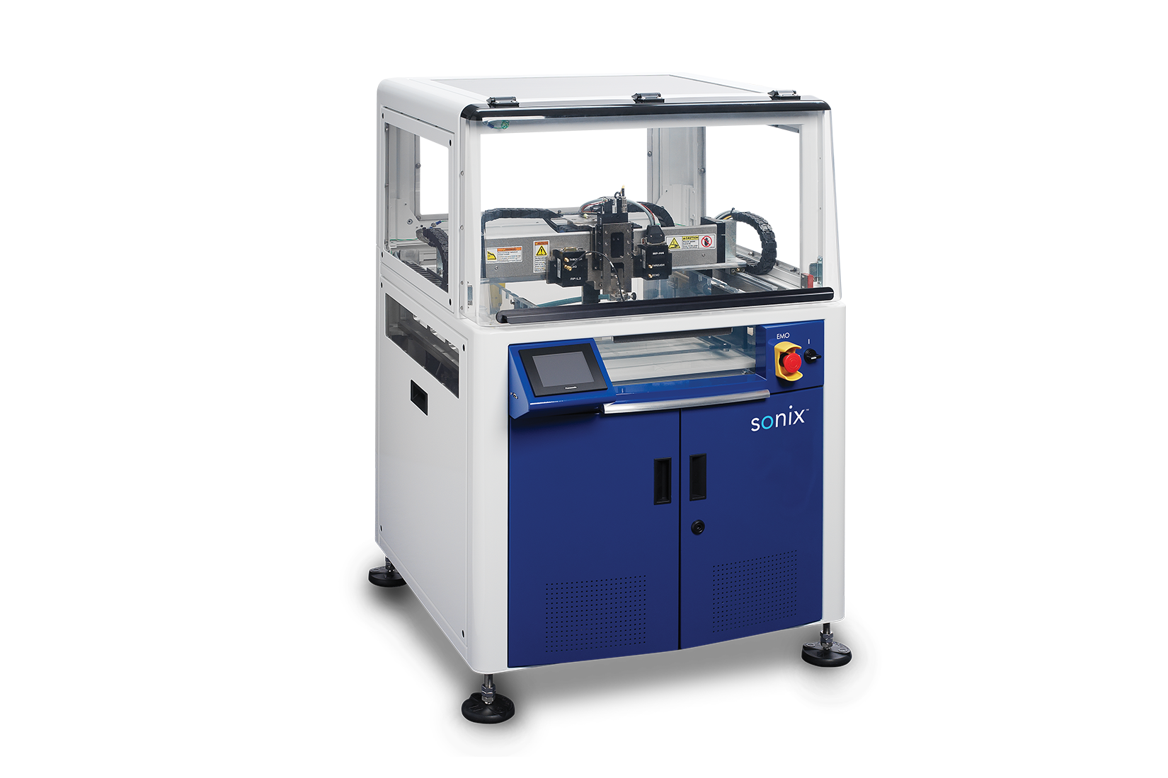
As devices become smaller and smarter, packaged semiconductor manufacturers are competing on their ability to deliver innovative form factors and materials. Sonix continuously advances our acoustic microscopy and analysis tools to clearly identify defects in the newest, most complex flip chip packages.
Sonix systems provide the image quality and throughput manufacturers of flip chip technology need to eliminate flip chip bonding defects at the process level and maximize inspection rates on the production line. Sonix provides automated tray scanning of individual flip chip packages and board-mounted flip chip technologies, with tools to optimize analysis of features such as:
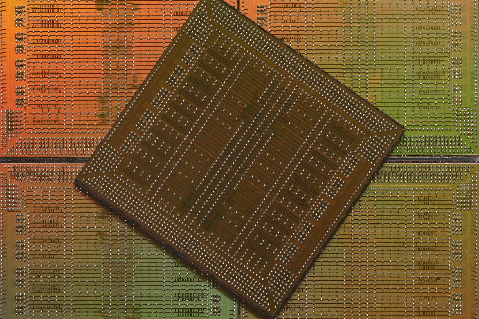
Learn advanced inspection techniques for Cu Pillars, molded underfill and stacked die package. Download our new white paper.
© 2024 Sonix. All Rights Reserved.