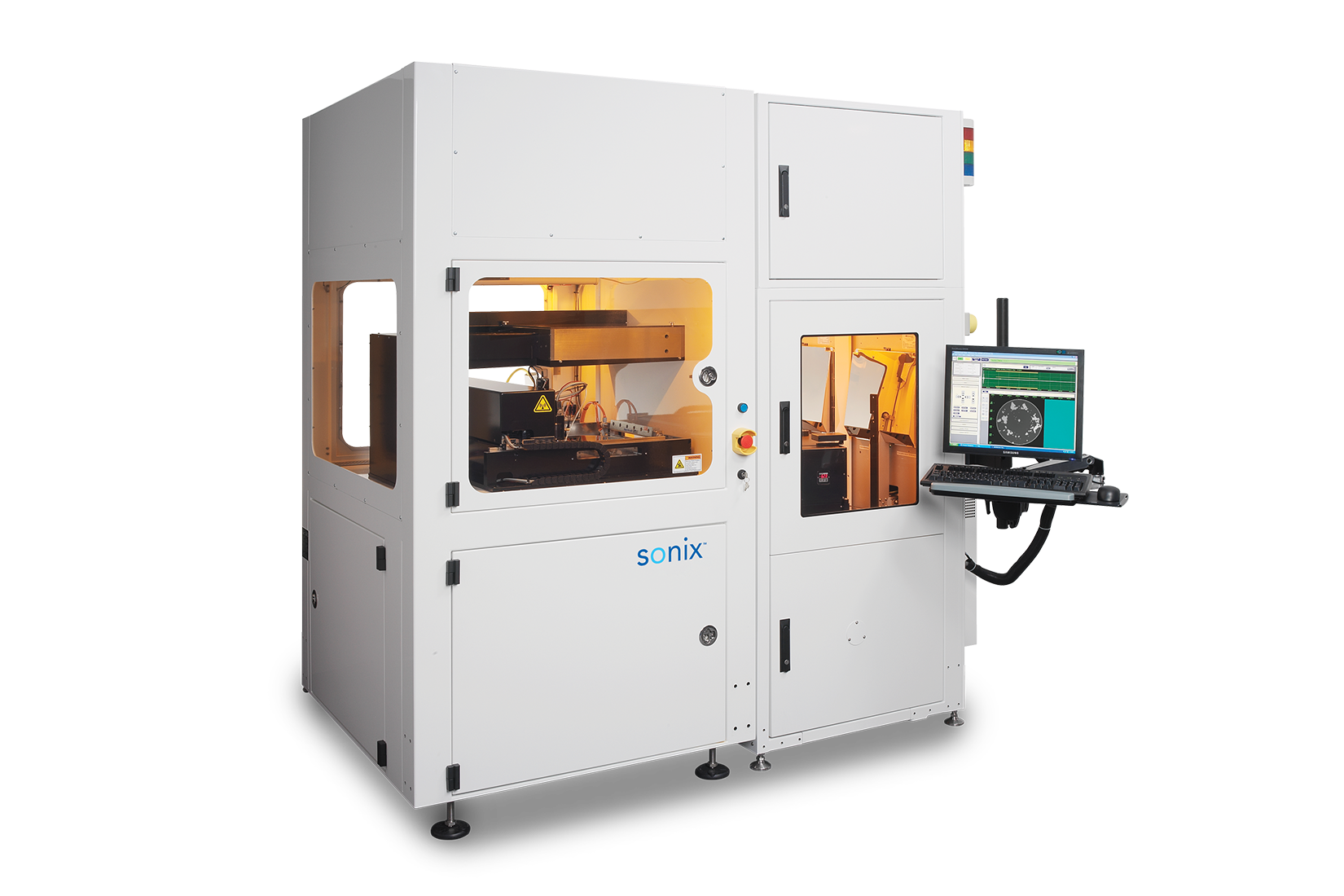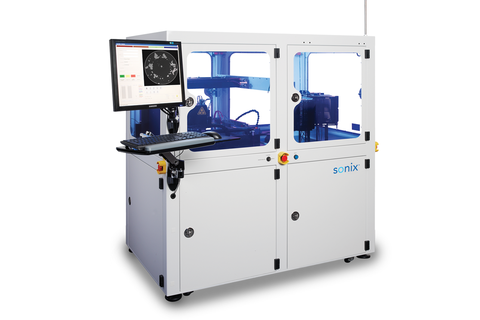
With increasing miniaturization and complexity, silicon devices depend on the quality of the wafer bonding process for long-term reliability. Electromechanical testing can’t detect wafer bowing, warping, micro-cracking, bonding gaps or contamination that may eventually lead to device failure. Sonix wafer inspection systems provide nondestructive testing (NDT) to detect gaps and voids of less than 0.1 micron, enabling superior diagnostic imaging for wafer bonding and device-level bond rings in silicon-on-insulator, anodic, metal-to-metal and other high-end bonded wafer applications. Defects can be precisely mapped as part of the wafer inspection process, so that good areas of the wafer can be salvaged to reduce scrap. Ultrasonic clarity to help improve wafer reliability and yield: that’s the Sonix difference.
Ultrasonics: The Best Choice
Optical inspection systems are widely used to verify proper structure, alignment and absence of contaminants prior to wafer bonding, but can’t reveal bonding defects that lie below the surface after wafer bonding. X-ray inspection systems can provide clear imaging of metallic features, but can’t clearly show bonding voids, delaminations, cracks and other air type defects. Infrared inspection doesn’t offer the image resolution needed to reliably detect defects smaller than about a half millimeter. Only ultrasonic inspection can provide the penetration and resolution required to clearly show defects at any wafer layer or depth, at scales measured in microns.
Sonix for Any Bonded Wafer Application
Advancements in wafer bonding have enabled new technologies that touch on every aspect of contemporary life. We can help you choose the right frequency, focal length and scan settings for any application, for example:
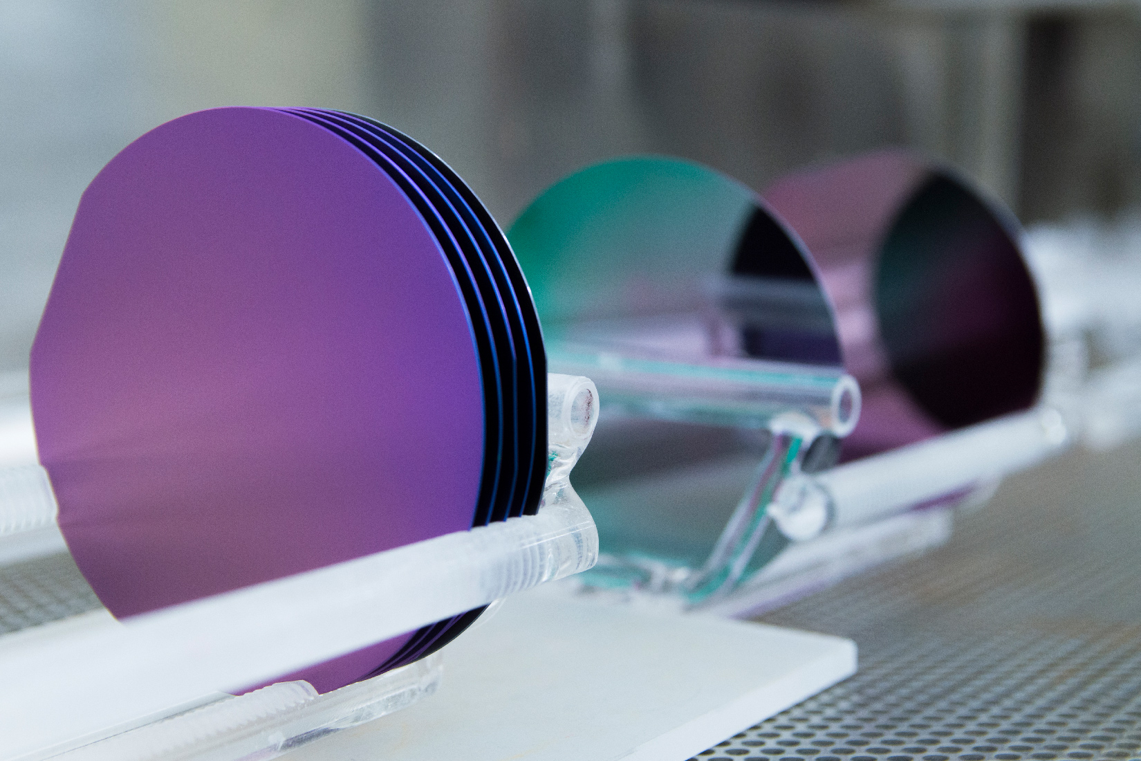
These techniques are used in the manufacture of microprocessors, high-performance radio circuitry, photonics, CMOS image sensors and microelectromechanical systems (MEMS) such as microphones, pressure sensors, accelerometers, gyroscopes, optical switches, microactuators, microscanners and more. Each industry, application and production environment brings its own set of challenges. At Sonix, we’re dedicated to helping you implement the inspection technologies and processes that are exactly right for your business.
| Bonded and Bumped Wafer | 103 KB | Acoustic inspection of bonded and bumped wafers has been given a lot of interest recently as advances in wafer manufacturing has generated a significant need to ensure wafer reliability. | DOWNLOAD |
© 2026 Sonix. All Rights Reserved.