Visualize the smallest subsurface features and defects in bonded wafers, packaged semiconductors and industrial materials. Scanning acoustic microscopy provides the nondestructive insight you need to make your products better.
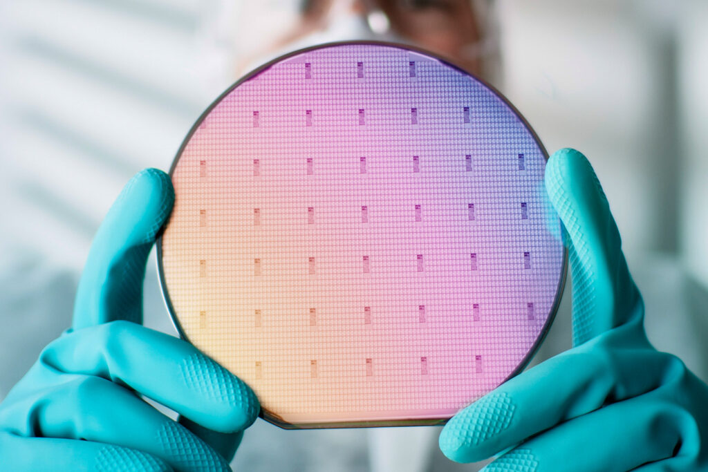
Inspect 100% of your production yield for microelectromechanical pressure sensors, microphones, gyroscopes, accelerometers and more. Sonix systems offer high-resolution scanning and production-speed throughput, with automated handling and sorting of approved and failed wafers. Get optimum spatial and depth resolution for any MEMS application. Read More About MEMS Inspection >
Looking for answers? If you don’t see what you need here, contact our support team with any product question or technical issue.
© 2026 Sonix. All Rights Reserved.