Sonix began business in 1986 in Springfield, Virginia, where our corporate headquarters still reside. We quickly grew to establish additional offices across the U.S. as well as in Europe, China, South Korea, Taiwan and Malaysia, with regional representatives in all the world’s major centers for wafer and packaged semiconductor manufacturing.
Our history is one of firsts, beginning with the industry’s first PC-based nondestructive testing system in 1987. In 1990 we introduced the first IC inspection system, and throughout the decade we brought to market innovations such as automatic inspection, TAMI and ICEBERG imaging software, wafer inspection and much more.
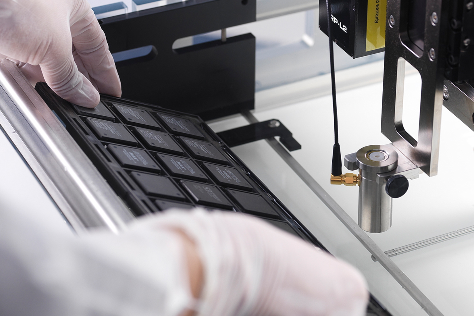
In the 21st Century, we’ve continued to grow our global footprint and advance our capabilities with Automated Wafer scanning for faster throughput, SDI enhancement for inspecting 3D architectures, MFCI for enhanced imaging of molded flip chips and other exclusive technologies. And we’ve built a service and support organization dedicated to collaborative problem solving to advance your business and technical capabilities.
Our history, and our future, is driven by your needs. As we work to build customer relationships, everything we learn helps us build better products and deliver better service.
Incorporation
First digital nondestructive imaging system
First Asia office
First IC inspection system
First automated JEDEC tray system
Introduction of TAMI imaging software
First wafer inspection system
Introduction of:
Patented Pulse Echo
Thru Transmission (PETT)
Introduction of Auto Analysis
First automated wafer inspection system
ISO 2001 certification
Introduction of Wave Form Simulator/Beam Emulator
ECHO platform and S-series transducers (35-75 MHz)
AutoWafer Pro, ECHO Pro and S-series transducers (110 MHz-UHF)
AutoWafer software, including MFCI (molded flip chip imaging), SDI (stacked die imaging), Flexible TAMI and waveform averaging
Introduction of 300mm SECS/GEM
© 2026 Sonix. All Rights Reserved.