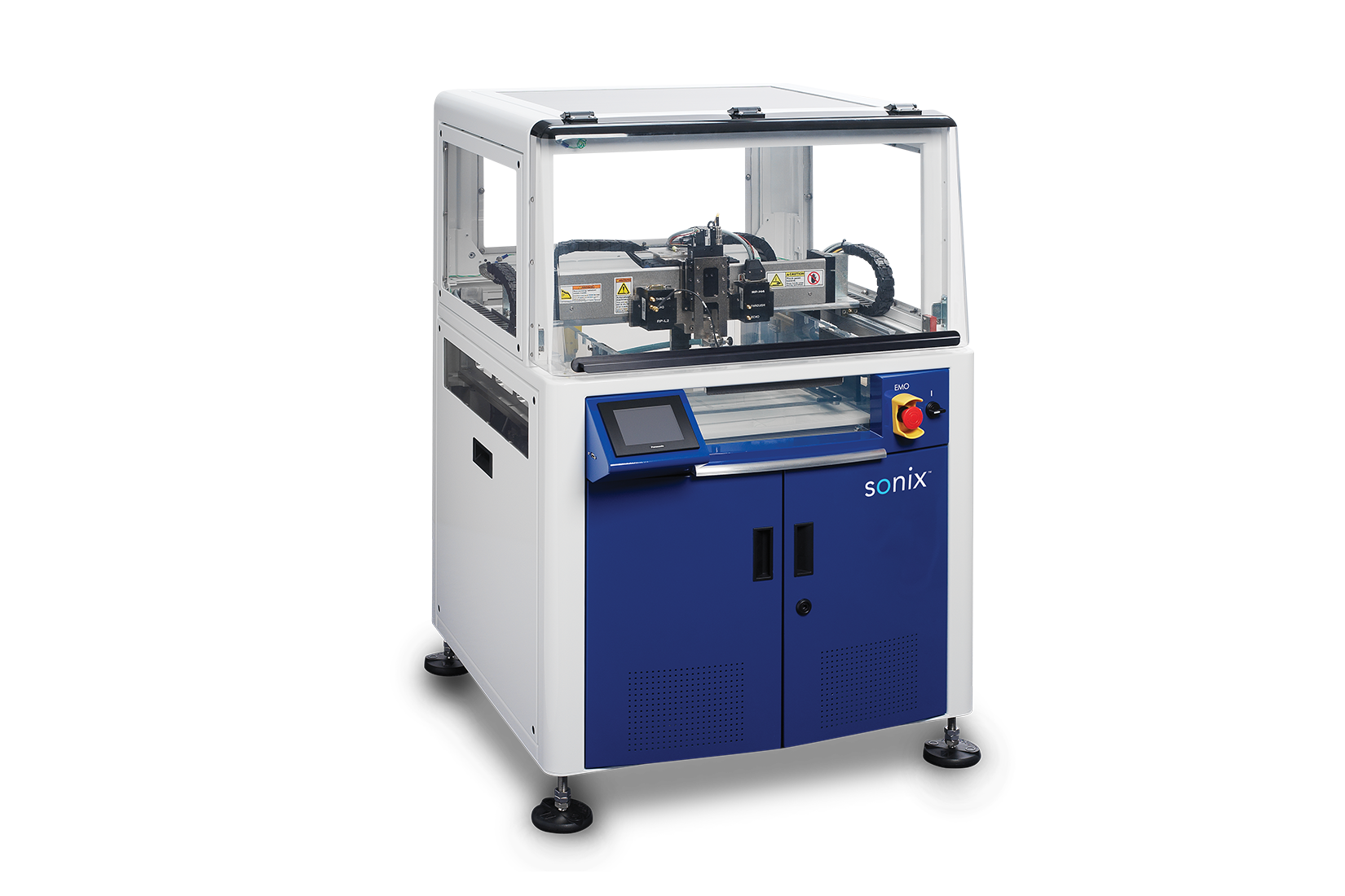
Chip scale packages (CSPs) allow for integration of greater functionality in a much smaller package. Today’s consumer devices require smaller and more powerful CSPs, with thinner materials and more complex layouts. As wafer packaging processes become more difficult and involved, the potential for chip package quality failures is a greater concern. Minimize quality risks in wafer level chip scale packages with Sonix solutions.
Sonix has the expertise to help you image specific interfaces of interest within the chip scale package, efficiently gathering the most useful data so you can maintain the multi-chip package throughput you need. With high resolution imaging of planar defects of less than 0.1 micron, Sonix systems identify and characterize:
| Chip Scale Packages App note | 125 KB | As the push for smaller and smaller packages has gotten stronger, chip scale packages have proven to be a valuable resource. | DOWNLOAD |
© 2026 Sonix. All Rights Reserved.